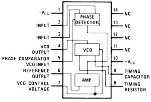
20+ ic 565 pll block diagram
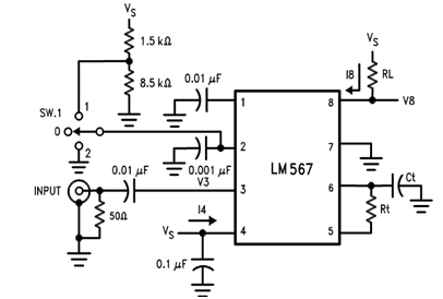
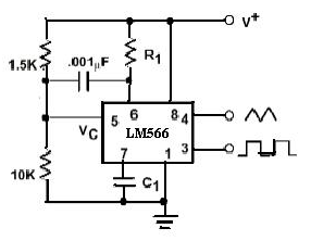
Phase Detector. The output frequency of the V CO is f o 12 4 R T C T where R T and C T are the external Resistor and Capacitor connected to pin 8 and pin 9.
Lm565 Ic Pin Configuration Specifications Circuit Its Applications
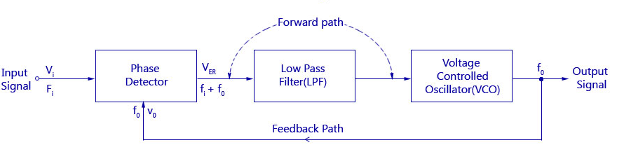
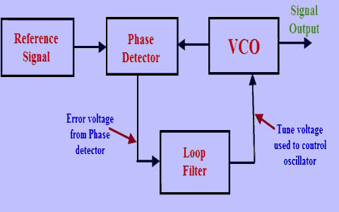
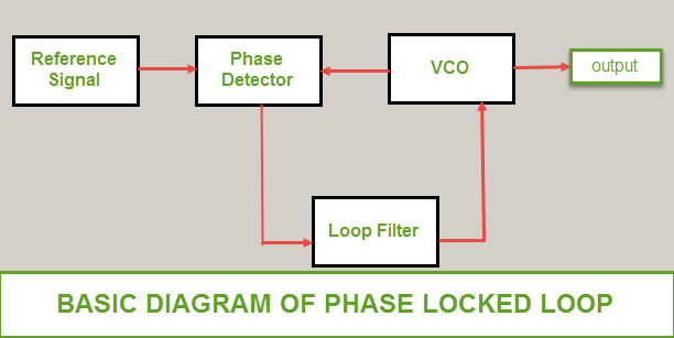
The block diagram of IC 565 includes a V CO in a feedback loop an amplifier a low pass filter and a.

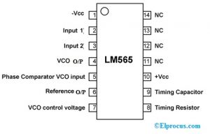
. LM565 IC Pin Configuration. The purpose of each pin is self. 1 The phase detector compares the input frequency fIN with the feedback frequency fOUT.
The important electrical characteristics of the 565. At the input of 565 the loop locks. Pin Configuration of PLL IC 565.
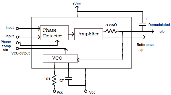
This IC includes 14-pins where each pin and its functionality are discussed below. The pin diagram of IC 565 is shown in the following figure. Basic Block Diagram Representation of IC 565 The signetics NESE 560 series is monolithic phase locked loops.
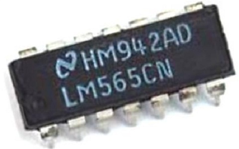
The output of 555 FSK generators is applied to the 565 FSK demodulator. Block diagram of LM565 PLL. It is a 14 pin Dual-Inline Package DIP.
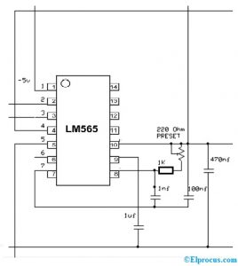
The SENE 560 561 ROHINI COLLEGE OF. 562 564 565 567 differ mainly in operating frequency range poser supply requirements frequency bandwidth adjustment ranges. The pin configuration n of the LM565 Phase Locked Loop IC is shown below.
The 565 IC is available as a14-pin DIP package. 565 Phase-Locked Loop Block diagram explanation. IC 565 is the most commonly used phase locked loop IC.
It consists of Figure b shows the block diagram of IC 565 Phase detector. Capacitive coupling is used at the input to remove dc line.
Monolithic Phase Locked Loop Linear Ic Questions And Answers Sanfoundry
Implementation Of Do Ota With Lm13700 Integrated Circuits Download Scientific Diagram
Lm565 Ic Pin Configuration Specifications Circuit Its Applications
Lm565 Ic Pin Configuration Specifications Circuit Its Applications
Phase Locked Loop Operating Principle And Applications
Voltage Controlled Oscillator Usage Of Vco Working And Application
Phase Locked Loop Operating Principle And Applications
Monolithic Phase Locked Loop Linear Ic Questions And Answers Sanfoundry
Phase Locked Loop Operating Principle And Applications
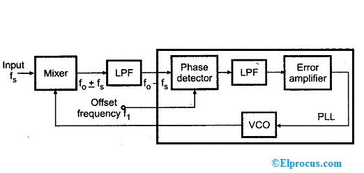
Frequency Translation Using Pll Working And Its Applications

Block Diagram Of The Phase Locked Loop Circuit Download Scientific Diagram

Block Diagram Of The Phase Locked Loop Circuit Download Scientific Diagram

Simplified Block Diagram Of The Global Car Radio Tuner Ic Download Scientific Diagram
Voltage Controlled Oscillator Usage Of Vco Working And Application

Block Diagram Of The Phase Locked Loop Circuit Download Scientific Diagram
Lm565 Ic Pin Configuration Specifications Circuit Its Applications

Pdf A Digital Phase Locked Loop Based Signal And Symbol Recovery System For Wireless Channel